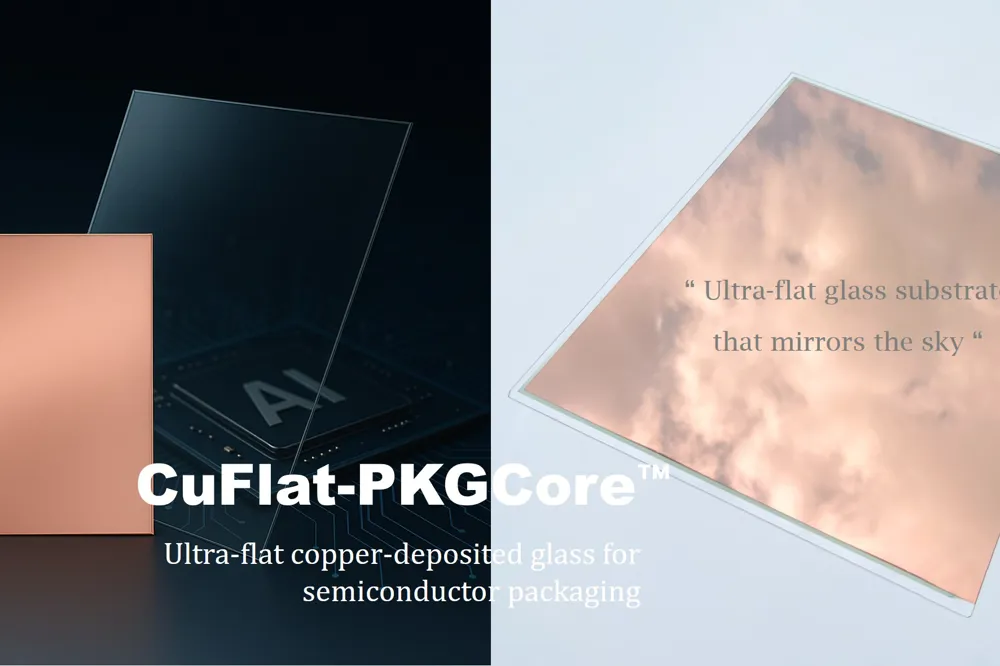
Ultra-flat copper-glass substrate for advanced chips such as AI accelerators – A material solution that reduces signal loss and maximizes the reliability of high-integration, high-speed chips by depositing copper on a semiconductor package substrate with atomic layer-level flatness.
HonoreeComputer Hardware & Components반도체 패키징구리 증착초평탄 유리고집적첨단 소재평탄도
CuFlat-PKGCore™: 반도체 패키징용 초평탄 구리 증착 유리
47
0
CIT Co., Ltd.
One-Line Product Definition
Problem Definition
As the circuit integration density of high-performance AI/5G semiconductors increases, even minute unevenness in the package substrate can cause signal distortion, heat generation, and defects.
Existing organic substrate + copper foil processes have rough copper surfaces and require multiple chemical processes for interlayer adhesion, leading to process complexity and environmental pollution issues. Furthermore, there are limitations in reducing substrate thickness, increasing the need for thinner and flatter substrates.
Key Differentiators
CuFlat-PKGCore™ achieves extreme flatness with a surface roughness of less than 3nm by depositing pure copper on a glass substrate at the single-crystal level without a seed layer, using CIT's Atomic layer epitaxy (ALE) technology [9]. This is more than 200 times smoother than the highest grade copper foil currently available, enabling the implementation of ultra-fine circuits as intended by semiconductor package designers.
It also does not oxidize up to 250℃, ensuring stable performance even in high-temperature environments. By replacing multi-step chemical processes with a single deposition step, it achieves a 3-4x increase in production speed and a 95% or greater reduction in carbon emissions/wastewater. In other words, the differentiation lies in the dramatically improved performance (↓ signal loss), reliability (high-temperature stability), production efficiency, and eco-friendliness.
Key Adopters
Semiconductor package substrate manufacturers and fabless companies (B2B) are the key customers. Companies developing ultra-high-speed, high-integration chips such as AI accelerators, data center chips, 5G communication chips, and autonomous vehicle chips can adopt this material to improve product performance.
Furthermore, it is expected to be supplied throughout the industry through partnerships with existing PCB substrate companies.
Scalability
The technology can be expanded not only to the semiconductor industry as a whole but also to various high-frequency/transparent conductor applications such as 5G antennas, transparent displays, and biosensors.
Currently, collaborations are underway with Korea, Japan (AGC Corporation), etc., and joint development is being pursued with global companies, making entry into the global market within sight [14]. However, while it may take time to enter the semiconductor material supply chain, the outlook is bright due to technology patents and securing initial demand.
Judges' Evaluation
It was evaluated as a material that will lead the paradigm shift in semiconductor packaging. It has been recognized for its technological prowess by winning the CES Innovation Award, and has also received rave reviews as "a small company that has solved the biggest problem of the AI era."
Market expectations are high for this innovation that challenges the limitations of microfabrication, but at the same time, realistic challenges such as manufacturing scale-up and mass production verification are also pointed out. Overall, the evaluation of technological completeness is very positive, and if adoption by major semiconductor companies occurs within the next 1-2 years, it is being noted for its potential to change the industry landscape rather than being underestimated.
Analyst Insights
⚠️ Impressive technology but market uncertainty – Expectations are high due to material innovation, but the success of the business will be determined by the adoption by large customers and the stabilization of mass production.
The award list data is based on the official CES 2026 website, and detailed analysis content is produced by USLab.ai. For content modification requests or inquiries, please contact [email protected]. Free to use with source attribution (USLab.ai) (CC BY)
댓글 (0)
댓글을 불러오는 중...