The world's first ultra-thin battery solution for extreme environments, designed for semiconductor manufacturing wafer sensors.
HonoreekoEmbedded TechnologiesAI 반도체웨이퍼 레벨 센서배터리 솔루션고진공 환경초박형 배터리MEMS 센서
Artenix™ AI
2
0
LiBEST Inc.
One-Line Product Definition
Problem Definition
In advanced AI semiconductor processes, sensors are used to monitor wafer conditions in real-time. However, the power supply technology to drive these sensors has stagnated for decades. Wired power sources cause process instability and particle generation due to cable vibration, and existing batteries cannot withstand high-temperature, high-vacuum, and strong electromagnetic environments, making them unsuitable for semiconductor processes. Consequently, while sensor technology has advanced, power supply remains a blind spot, impossible to implement under extreme conditions such as vacuum and plasma.
Key Differentiators
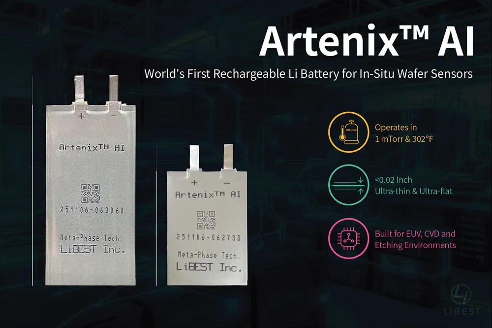
Artenix AI is the world's first battery specifically designed for semiconductor processes, filling this gap. It is designed with gas and dust-free materials and structures to ensure stable operation in extreme environments, including ultra-high vacuum of 1 mTorr, rapid thermal cycling, and strong electromagnetic interference.
As an ultra-thin battery with a thickness of less than 0.6mm, it seamlessly integrates into wafers or equipment and has almost no thermal expansion, thus not affecting process precision. Furthermore, it operates in a vacuum without leakage due to its meta-phase electrolyte which contains no liquid electrolyte, and maintains performance even after thousands of charge-discharge cycles. In other words, its key differentiation lies in providing reliability optimized for the process environment in spaces where existing batteries are impossible, thereby enabling complete wireless operation of sensors and continuous collection of process data.
Key Adopters
The main customers are semiconductor manufacturing companies (fabs) and equipment manufacturers that supply them. It is structured as a B2B supply of parts/solutions, with global foundries, OSATs (outsourced semiconductor assembly and test), and equipment manufacturers being the primary adopters of this technology.
It is expected to be used directly by applying it to sensor wafers in their production lines, or by equipment manufacturers embedding it in their equipment for sale. Ultimately, it can affect the entire semiconductor process monitoring industry, and adoption may be discussed in the form of national projects or large enterprise consortiums (B2G nature). Although general consumers do not directly encounter it,Business-to-Business (B2B)It is a solution that enters the semiconductor industry supply chain.
Scalability
Currently, the focus is on the specialized area of semiconductor production processes, but since this is a global industry, it can spread on a global scale once it becomes a standard. Furthermore, depending on the technology application, there is room for expansion into other fields that require extreme environment sensors, such as aerospace and defense.
However, initially, it is limited to a niche B2B market tailored to the process environment, so standardization and securing a competitive advantage are necessary for significant market expansion. In terms of regulations, there are no special barriers other than certification for battery safety, and if it is adopted as a semiconductor industry standard, it can have ripple effects into other industries.
Judges' Evaluation
Industry experts say this product"fills the last hidden puzzle of the AI semiconductor era."The CES Innovation Award is an unusual achievement for innovation in the materials and battery fields, and it is analyzed that LiBEST has triggered a standard competition for global semiconductor process power technology.
Regarding the technology itself,it is highly praised as a "groundbreaking solution that solves a problem that has not been solved for decades,"and it has received attention as it was led by a Korean startup. On the other hand, regarding marketability, there is a cautious view that there is a risk of commercialization because the target market is limited and competition with global companies with huge capital is expected. Overall, technological innovation is rated very highly, and expectations are high for future moves as PoC and collaboration discussions have begun with actual global semiconductor companies.
Analyst Insights
⚠️ Excellent technology, but market adoption is uncertain
The award list data is based on the official CES 2026 website, and detailed analysis content is produced by USLab.ai. For content modification requests or inquiries, please contact contact@uslab.ai. Free to use with source attribution (USLab.ai) (CC BY)
댓글 (0)
댓글을 불러오는 중...